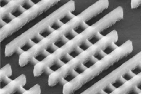
What's the News: The foundation of modern electronics, silicon transistors are miniature on/off switches that regulate electric current. This week, Intel demonstrated a new transistor design that's being hailed by Intel as one of the most radical developments in transistors since the advent of integrated circuits of the 1950s. By adding tiny, vertical fins to normally flat transistors, Intel's new Tri-Gate transistor allows for faster, smaller, and lower-voltage computer chips. "We've been talking about these 3-D circuits for more than 10 years, but no one has had the confidence to move them into manufacturing," chip-manufacturing specialist Dan Hutcheson told The Wall Street Journal.How the Heck:
Engineers added a fin-shaped structure to the part of the transistor that acts as a conducting channel for electrons; with the extra depth, more current flows through the transistor.
They also designed the gate, or the component that turns the current flow on and off, so that it surrounds the fin on all three sides, more effectively stanching current from leaking when it's off. All told, the new 3D structure should allow gadgets to guzzle half the power than Intel's current product line. "That is an unprecedented gain," Intel fellow Mark Bohr told The Wall Street Journal. "We've never achieved that kind of performance gain at low voltage."
When combined with Intel's new manufacturing process---changing from 32-nanometer chips to 22-nanometer ones---the company says the new transistors work 37% faster when chips are in low-voltage mode, and 18% faster in high-voltage mode.
As CRN’s Edward Correia notes, “With the triple-gate transistor, Intel has reinvented the technology that powers every computing device---indeed, all of today's electronics---and in doing so, has broken the size restrictions currently inherent in today's microprocessors.” He says the really significant thing is how Intel has “has developed a process for mass-producing the circuits in a process that's 22 billionths of a meter thick, about a third thinner than the 32-nm process it uses for Sandy Bridge microprocessor architecture (a human hair is about 100,000-nm thick).”
What's the Context:
The 3D approach Intel has now developed was first mentioned in a series of research papers in 2002. Its rivals have been exploring similar designs, but Intel is the first company with plans of shifting its entire production to the 3D structure.
Intel's new Tri-Gate transistors are expected to add only upwards of 3% cost to the production of each wafer---a small amount given its significant strides in performance.
The idea of building upward instead of outward is just one of many ideas for better chips that companies have thrown around in recent years.
Not So Fast:
Globalfoundries, a production service that shares research and development with IBM and Samsung, snubbed the transistor breakthrough, saying that "we don't see the need" for technologies like 3-D transistors at the current time. Their focus is just to increase performance by shrinking their transistor manufacturing to the 22/20nm scale.
In the smartphone market, Intel is still getting trumped by its competitors because its chips consume more energy, leading to lower battery life. It’s too early to tell whether the new 22-nanometer scale Tri-Gate transistor, with its low-voltage abilities, will let Intel gain ground in the mobile market.
The Future Holds:
Intel plans on completely shifting its manufacturing process to the new transistors in the near future. They'll start mass-producing the 3D transistors later this year, with high-end desktop computers rolling off the shelves in early 2012.
Building true 3D chips, with layers of transistors built on top of each other, still hasn't been achieved. Adding an entire second layer of transistors (and eventually even more to stack them into cubic chips) is the "hotly-pursued goal of the industry."
Images: Intel


