We have completed maintenance on DiscoverMagazine.com and action may be required on your account. Learn More

Beyond Graphene, a Zoo of New 2-D Materials Are Being Created

The Crux
By Andy Berger
Jul 17, 2015 7:00 PMNov 20, 2019 1:47 AM
Boron-nitride-hexagonal-side-3D-balls-1024x505.png

Newsletter

Sign up for our email newsletter for the latest science news
 

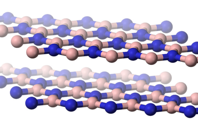
Two alternately stacked layers of hexagonal boron nitride. Nine years ago, Joshua Robinson was approached by his then-advisor with news of a discovery that would end up transforming his career, and much of materials science. “I saw this crazy talk about 2-D graphite,” he recalls his adviser saying. The adviser was referring of course to graphene, the first material to exist as truly two-dimensional: only a single atom thick. Back in 2006, the physics community was just beginning to wrap its mind around how a 2-D material could even exist. Fast forward to 2015. The realization that materials can be thinned down to the absolute limit of a single atom is spreading, both throughout the world and across the periodic table. Researchers are learning that 2-D isn’t just for the carbon atoms of graphene. Different elemental combinations can lead to fascinating new science and applications. Robinson is now associate director for Pennsylvania State University’s Center for Two-Dimensional and Layered Materials, a center with 20 faculty and over 50 students dedicated to uncovering the fundamental properties of this new zoo of 2-D materials. It is one of many such centers around the world. And as scientists continue to create new 2-D materials there’s a palpable frenzy to characterize their surprising electronic, optical, and mechanical properties. The excitement stems from the fact that materials shaved down to only a few atoms act very differently from their so-called “bulk” or 3-D version. Quantum effects begin to take hold as the electrons in the material are squeezed into that impossibly thin layer. And, being flexible, 2-D materials could bring those unique electrical properties to all sorts of new applications – from bendable touch screens to wearable sensors.

Beyond Graphene

The granddaddy of 2-D materials, graphene, was first isolated in 2004. That discovery sparked intense activity in fundamental research labs everywhere. However, graphene’s commercial success has not yet matched its hype. It has only trickled out to a few niche products so far, such as weight-optimized tennis rackets and efficient light bulbs. Graphene’s major weakness is its lack of a band gap, which is what makes silicon and other semiconductors so useful for digital electronics. A band gap allows electrical conduction through a material to be turned on and off, which is key for building a transistor – the electronic switch that speaks the 1s and 0s of digital code. And the huge excitement around graphene was also cause for worry – would the graphene well dry up? “Everyone is working on it, everything is being done,” recalls Roland Kawakami, a physics professor at the Ohio State University. As its behavior becomes more fully understood and its potential applications explored, interest in graphene has indeed begun to plateau. Since 2012 the number of presentations about graphene at the American Physical Society’s annual conference has stayed flat. Meanwhile many of graphene’s early adopters, like Kawakami, have expanded into the 2-D materials beyond graphene. Judging by the same measuring stick – APS presentations – these materials are just beginning to heat up.

A Wealth of Properties

The first of graphene’s descendants to attract attention was molybdenum disulfide (MoS2­­­), a silvery black solid that looks similar to graphite. In 2010, the group of Tony Heinz at Columbia University showed that when thinned down to a single monolayer, MoS2 becomes a highly efficient light source, 10,000 times brighter than its bulky 3-D cousin. This could make it very useful for ultra-efficient LEDs, or, conversely, for transforming light into electrical energy in fiber-optic networks or solar cells. The light-electricity conversion in MoS2 is made possible by that elusive quality which graphene lacks: a band gap. Andras Kis demonstrated in 2010 that single-layer MoS2 could indeed be used to create a transistor. As silicon fights to keep pace with ever-shrinking devices, MoS2 might be perfect for ultra-small, low-power transistors. These findings have spawned growing interest in the cousins of MoS2. Other so-called transition metal dichalcogenides, or TMDs, in their 2-D form exhibit a slew of different properties, from semiconducting to metallic to superconducting. Some of them even behave as topological insulators: most of the material is insulating, while only the very perimeter conducts electricity. With this breadth of new properties, Kawakami says, “you start seeing people in other fields start to get interested.” TMDs are attracting attention from researchers as far and wide as optics, electronics, superconductivity, and semiconductors.

A 2-D transition metal dichalcogenide. Credit: 3113Ian

In the Family

The other major class of 2-D materials more closely resembles graphene. Silicon, germanium, and tin come from the same chemical family as carbon. But, while graphene is quite content as a perfectly flat 2-D layer, silicene, germanene, and stanene prefer a corrugated, slightly 3-D structure. This means that they easily make chemical bonds with molecules above or below the 2-D plane, giving chemists a new way to tailor the properties of the sheet. For instance germanene, like graphene, has no band gap, but by bonding a hydrogen atom to each germanium atom, chemists can create one. And, by using a palette of different chemicals, one single sheet can have splotches of different properties. Joshua Goldberger, a chemist at OSU who co-leads their 2-D efforts with Kawakami, envisions using such patterning to create a chemically defined 2-D electronic circuit. However, these materials’ affinity for chemical bonding is a double-edged sword – it makes the “enes” unstable in air. The first silicene transistor lasted just minutes. Researchers are actively pursuing ways to prevent this degradation, either by sandwiching the 2-D layer between protective insulating sheets, or by bonding inert molecules to the layer. Finally, phosphorous, though not quite in the carbon family, has shown some promising capabilities in its 2-D form, phosphorene. It exhibits a natural band gap like the TMDs, but its electrons are still able to zip about with ease, like graphene. And an intriguing quality of phosphorene is that simply stretching it can change the size of its band gap. That could lead to color-tunable lasers and light sensors.

Germanene on the outermost layer of a Ge2Pt crystal.

Combining Flavors

But, perhaps counterintuitively, the real breakthroughs with 2-D materials could come from layering them into 3-D stacks. Mixing and matching different layers can create interesting, unforeseen properties. “When we put our peanut butter and our jelly together, it’s not just a peanut butter and jelly sandwich,” Robinson says. “Now all of a sudden it’s a chicken.” Robinson’s team just published a study in which they stacked two different TMD layers onto graphene. This triple-decker behaved in a wholly unpredicted way, showcasing what’s called negative differential resistance – applying more voltage to the device resulted in less current flowing through it. That property could be useful for next-generation electronics but until now has been a challenge to accomplish at room temperature. With so many 2-D building blocks to choose from, every stack has the potential to surprise scientists. “And that’s the really exciting part, because there is a potential for some kind of property… that’s going to completely invent a new application,” Robinson says. There is a definite sense that the field is being driven more by youthful creativity than the instruction manual of prior experience. And that instruction manual has proved little help in the brave new world of 2-D materials. For example, much of the initial hype surrounding graphene pertained to electronics and the potential to dethrone silicon. “Silicon still is king, and so much brainpower has gone into silicon. Trying to replace silicon is not the be-all, end-all strategy,” explains Goldberger. Instead, researchers are tinkering and testing, and expecting surprises. At a recent 2-D workshop, Robinson recalls, “There was no one that stood up and said ‘I know what the killer app is’, because we’re still just trying to figure out what this stuff can really do.” It’s hard to overstate scientists’ hopes for the breakthroughs yet to come. “For my generation, 2-D materials is it,” says Kawakami. “Everything that you try is just a new thing.”

1 free article left
Want More? Get unlimited access for as low as $1.99/month

Already a subscriber?

Register or Log In

1 free articleSubscribe
Discover Magazine Logo
Want more?

Keep reading for as low as $1.99!

Subscribe

Already a subscriber?

Register or Log In

More From Discover
Recommendations From Our Store
Shop Now
Stay Curious
Join
Our List

Sign up for our weekly science updates.

 
Subscribe
To The Magazine

Save up to 40% off the cover price when you subscribe to Discover magazine.

Copyright © 2024 Kalmbach Media Co.